
Although not directly a change to any manufacturing techniques, one of the easiest methods manufacturers have found to increase their module performance is using a larger wafer size. Traditionally, mono-crystalline wafer sizes of 156 mm side length cut from a 200 mm diameter ingots have been used for over a decade. These wafers are known as type M0.
With wafer manufacturers pushing the size of the silicon ingots, 2 different types of wafers were produced, M1 and M2. With only a marginal increase in side length being 156.75 mm, their differences lie in the ingots they were cut from. M1 wafers are cut from ingots of diameter 205 mm whereas M2 wafers are cut from ingots of diameter 210 mm.
Although these wafers are only 0.75 mm longer in side lengths to the M0, the larger ingot sizes allow the wafer edges to be increased such that there is an increase in surface area in the corners. The M1 wafers gain an area of 97.33 mm2, obtaining an increase in the surface area of 1.63% compared to the M0 wafer. Furthermore, the M2 wafers gain an area of 131.33 mm2, obtaining an increase in surface area of 2.25% compared to the M0 wafer.
Putting this into perspective, a solar cell architecture of 19.95% efficiency using the M2 wafer format will show a 0.1 W power gain compared to M0. Therefore, larger ingot sizes allow for monocrystalline wafers to be less “pseudo” square, increasing the resulting wafer size and hence the amount of light that could be captured.
The major advantage of M2 wafers is that there is almost no changes required in the manufacturing line from M0 to M2 wafers, making this advancement in PV module design easy and cheap. M2 wafers became a standard in 2018 due to this ease in change. Similarly, with multicrystalline silicon wafers, simply cutting them at 156.75 mm side lengths is simple as they are already intrinsically square.
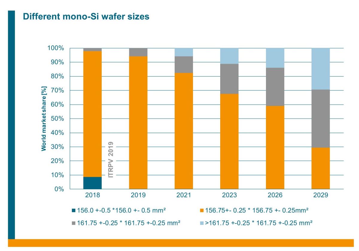
Although M2 wafers are easy to integrate, even larger wafer sizes are beginning to be used to obtain 400 W plus modules. JinkoSolar began producing modules with 158.75 mm side length in 2018, LG went even further with 161.75 mm in as early as 2017 whereas Canadian Solar pushed their multicrystalline technology with 166.75 mm side length cells. The 166.75 mm (or M6) wafers boast an increase of 12% surface area to M2 wafers making the technique of larger wafer formats a very cost-effective method for more high power PV modules. LONGi even began using M6 monocrystalline wafers.
Aside from more surface area, these larger wafer formats are also being used in other advanced module manufacturing techniques. An example is Canadian Solar’s 430 W module with PERC cells made from M6 wafers with multi busbars (MBB) and half cell format. However, the handling tools required to transport such larger wafers must be adapted or changed to suit the change from traditional M2 wafers to M6, which is an expensive adaptation compared to moving from M0 to M2 wafers.

Another benefit of larger wafer formats is making 6 busbars more viable when compared to 5 busbars. In more traditional wafer formats, the gains observed in 6 busbars compared to 5 busbars were not very significant. However, with larger wafers, the larger surface area that electrons must travel across makes the reduction is losses significant enough for manufacturers to opt for 6 busbars tools. Although MBB is not the easiest for manufacturers to integrate, this technology will allow the use of solar cells of various sizes.
Finally, both wafer and equipment manufacturers are still pushing ahead with the introduction of the M12 wafer by Zhonghuan Semicondutor, boasting a side length of 210 mm. With equipment manufacturers also following suit and adapting their technology to process such wafer sizes, the benchmark for larger wafer formats for higher power rated modules will consistently be challenged.
